Atomic scale materials "softer" or "harder"
The physical and chemical properties of atomic scaled-materials have been reported to be sensitive to the atomic configuration. However, such structural dependence has been understood rarely because of lack of experimental results. For example, the
Young's modulus of metal contacts have been expected to increase or decrease with decreasing the size, but the origin of such size dependent mechanic properties has not been understood. We challenge to solve such nanomechanical issues by development a special TEM holder equipped with a force sensor (in-situ TEM observation).
Development of a specific "in-situ" TEM holder
"Development of original equipment"
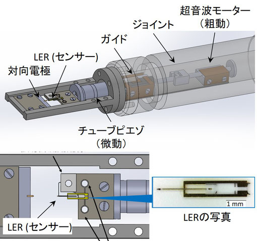
In order to clarify the mechanical properties of atomic scale materials, it is necessary to obtain the shape and crystal orientation of the nanomaterial at the same time as the mechanical
measurement (value of the force applied to the material or spring constant of the material). However, there is no such device, so we will develop an original
experimental equipment.
1. Design using 3D CAD
2. Order parts
3. Assemble the parts
4. (In some cases) Programming for controlling the equipment.


Nano electrical devices like atomic switch have been attracting interest. As the related research, electrical transport or mechanical properties of metal nano-contact become important issue. Although the mechanical properties of metal nano-contac are closely related to the contact structure, they have been rarely clarified because of lack of the suitable experimental equipment.
We developed the TEM-AFM holder equipped with a force sensor (one of the techniques used in atomic force microscopy (AFM)). By using this, we can measure spring constant of the contact simultaneously with observing its structure.
As shown in "a" to "d" in the left figure, the spring constant become smaller, while it gets narrower. In this way, we can get Young's modulus of the contact, indicates strength of the contact.

"Measure strength of platinum nano contacts"
The left figure shows time evolution of electrical conductance and spring constant of the platinum nanocontact while observing it. As shown by the black line, the electrical conductance changes
stepwise and finally becomes 0 (the contact breaks). The nanocontact become thinner while repeating cycles of elastic and plastic deformation, which correspond to the flat area and step
change, respectively. The spring constant also changes in a similar manner to electrical conductance, but the stepwise change is somewhat dull.
Compared with the TEM image, the platinum nanocontact shows relatively long plateau before breaking.