Structure-dependent electrical conduction
Much efforts have been devoted to development of nanodevices that are more compact and have higher performance (lower power consumption) than current semiconductor devices. Two-dimensional substances (sheets consisting of a single layer of atoms) are drawing attention as materials for such nanodevices, and graphene can be said to be a representative one. Various interesting theoretical predictions have been made about the electrical conductivity properties of graphene, but it has not been fully verified in experiments. The reason for this is that the electrical conductivity of graphene is sensitive to atomic arrangement. In other words, experimental verification requires technology that can simultaneously measure atomic arrangement and electrical conduction. In our laboratory, we are developing such a measurement method and trying to clarify the electrical conduction properties of graphene nanoribbons.
Discovery of graphene switch
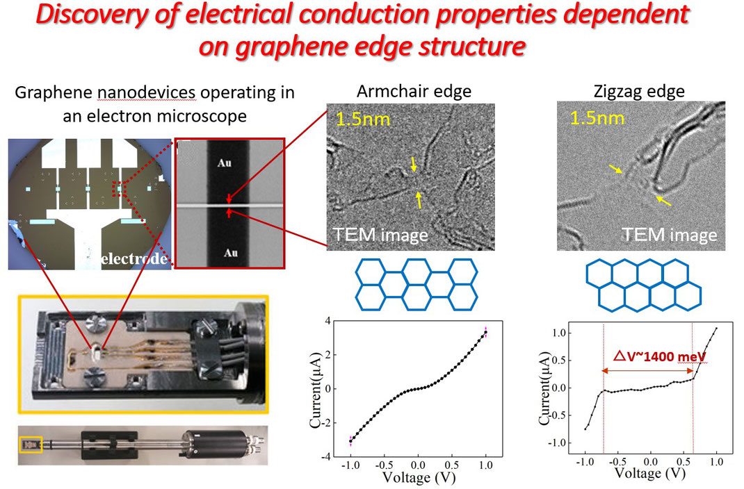
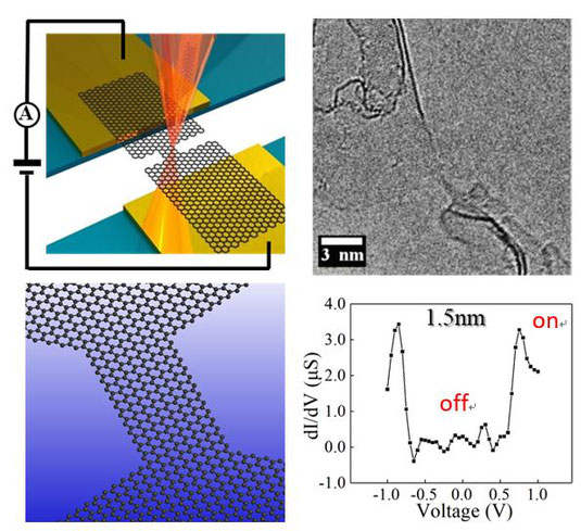
Researchers at Japan Advanced Institute of Science and Technology (JAIST) have successfully measured the current-voltage curve of graphene nanoribbons (GNRs) that were suspended
between two electrodes. Measurements were performed using transmission electron microscopy (TEM) observation. Results revealed that, in contrast to the findings of previous reports, the
electrical conductance of GNRs with a zigzag edge structure (zigzag GNRs) abruptly increased above the critical bias voltage. This finding is worth noting because the abrupt change in these GNRs
can be applied to switching devices, which are the smallest devices in the world.
The electrical structure of GNRs have been systematically investigated through theoretical calculations. Studies have reported that both zigzag and armchair GNRs exhibit
semiconducting behavior below several nm in width, although the origin of the energy gap is different. On the other hand, the electrical transport properties have rarely been calculated owing to
the non-equiribrium calculations required. In 2009, Nikolić et al. predicted that sharp increments in electrical conductance would occur for extremely thin and short zigzag GNRs as the
magnetic-insulator–nonmagnetic-metal phase transition occurs above a certain bias voltage [Phys. Rev.B 79, 205430 (2009)]. The obtained experimental results correspond closely to the results of
this non-equilibrium calculation.
A research team led by Ms. Chunmeng LIU, Professor Yoshifumi OSHIMA and Associate Professor Xiaobin ZHANG (now of Shibaura Institute of Technology) has developed a special in situ
TEM holder and a GNR device for TEM observation. This combination is aimed at clarifying the relationship between the edge structure of GNRs and electrical transport properties. Ms. Liu, the
doctoral student of JAIST, said, “The fabrication process of our GNR device is much more difficult than the conventional one because we need to make very narrow GNR which should be stably
suspended between both electrodes.” She reviewed the literature focused on the fabrication process of GNR devices and verified their process en route to establish her original fabrication method.
Assoc. Prof. ZHANG said, “We were really happy to see that the I–V curve obviously changed when changing the edge structure to zigzag. I suppose we have encountered new possibilities for graphene
nanoribbons.” The team has successfully performed the in situ TEM observation of extremely narrow GNRs, and they plan to continue identifying electrical transport properties of these GNRs which
are sensitive to the edge structure.
###
This research was supported by the research grants from the Sasakawa Scientifc Research, the Izumi Science Foundation, and the Iketani Science Foundation. C. Liu gratefully acknowledges the China
Scholarship Council (No.201808050001).
Development of a specific "in-situ" TEM holder
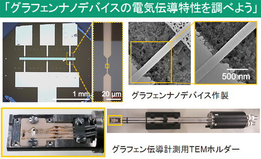
The upper left figure is a photograph of electrodes (3 places) made using electron beam lithography. These electrodes are designed on a 3mm diameter TEM grid. The next figure is an enlarged view of one electrode. There is a gap at the center of the electrode, and the right figure is a TEM image near the gap. As shown by this TEM image, the gap distance is very short, less than 100 nm. By suspending materials such as graphene to this gap, it is possible to observe its structure and measure the electrical conductance properties at the same time. The figure below is a photograph of "TEM holder for graphene electrical conductnce measurement", which can observe TEM by placing the fabricated TEM grid.